- 您现在的位置:买卖IC网 > Sheet目录3841 > PIC18LF66K80-I/PT (Microchip Technology)MCU PIC ECAN 64KB FLASH 64TQFP
2010-2012 Microchip Technology Inc.
DS39977F-page 135
PIC18F66K80 FAMILY
7.5
Writing to Flash Program Memory
The programming blocks are 32 words or 64 bytes.
Word or byte programming is not supported.
Table writes are used internally to load the holding regis-
ters needed to program the Flash memory. There are
64 holding registers for programming by the table writes.
Since the Table Latch (TABLAT) is only a single byte, the
TBLWT
instruction may need to be executed 64 times for
each programming operation. All of the table write oper-
ations will essentially be short writes because only the
holding registers are written. At the end of updating the
64 or 128 holding registers, the EECON1 register must
be written to in order to start the programming operation
with a long write.
The long write is necessary for programming the inter-
nal Flash. Instruction execution is halted while in a long
write cycle. The long write is terminated by the internal
programming timer.
The EEPROM on-chip timer controls the write time.
The write/erase voltages are generated by an on-chip
charge pump, rated to operate over the voltage range
of the device.
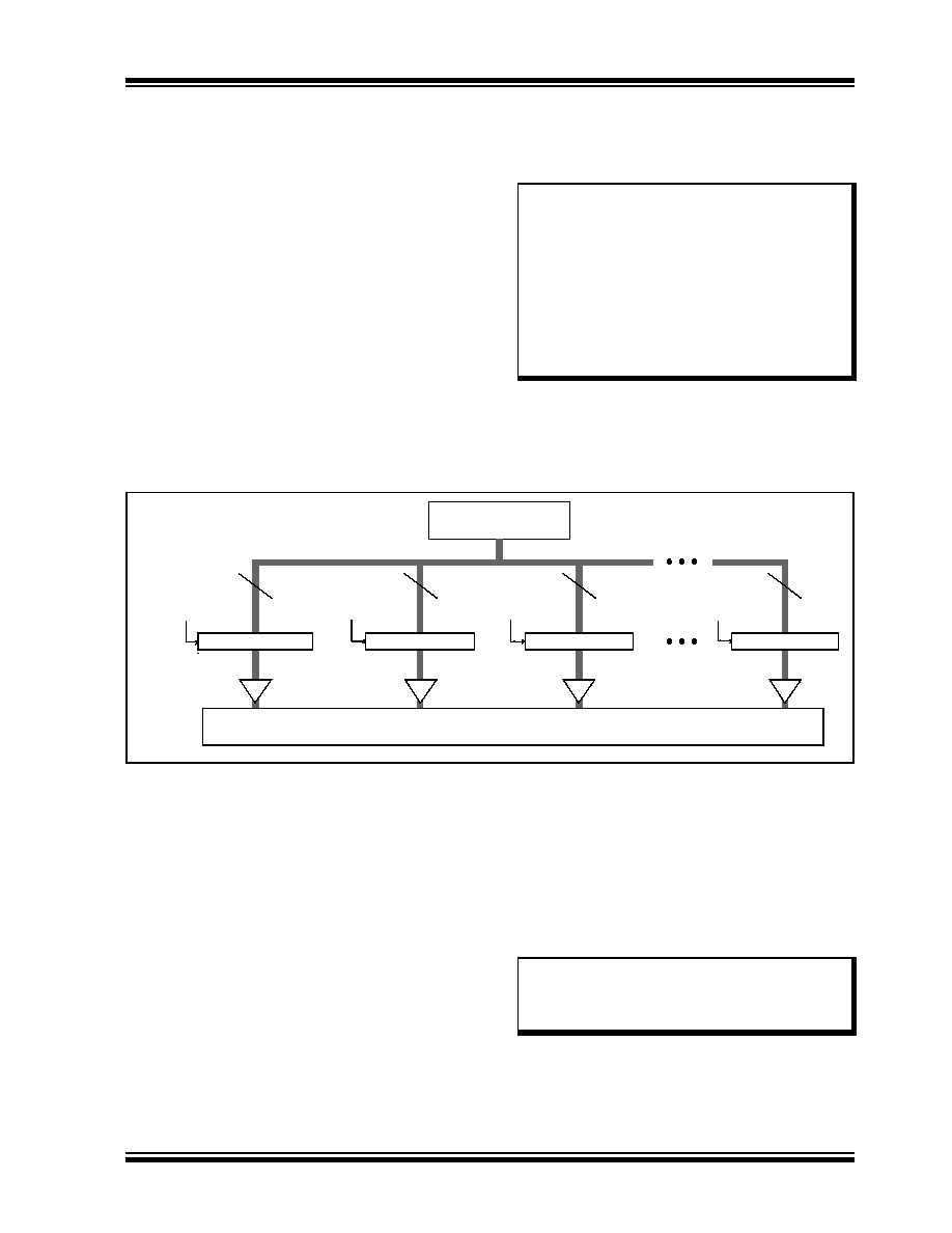
FIGURE 7-5:
TABLE WRITES TO FLASH PROGRAM MEMORY
7.5.1
FLASH PROGRAM MEMORY WRITE
SEQUENCE
The sequence of events for programming an internal
program memory location should be:
1.
Read the 64 bytes into RAM.
2.
Update the data values in RAM as necessary.
3.
Load the Table Pointer register with the address
being erased.
4.
Execute the row erase procedure.
5.
Load the Table Pointer register with the address
of the first byte being written.
6.
Write the 64 bytes into the holding registers with
auto-increment.
7.
Set the EECON1 register for the write operation:
Set the EEPGD bit to point to program memory
Clear the CFGS bit to access program memory
Set the WREN to enable byte writes
8.
Disable the interrupts.
9.
Write 55h to EECON2.
10. Write 0AAh to EECON2.
11. Set the WR bit. This will begin the write cycle.
The CPU will stall for the duration of the write for
12. Re-enable the interrupts.
13. Verify the memory (table read).
An example of the required code is shown in
Example 7-3 on the following page.
Note:
The default value of the holding registers on
device Resets and after write operations is
FFh. A write of FFh to a holding register
does not modify that byte. This means that
individual bytes of program memory may
be modified, provided that the change does
not attempt to change any bit from a ‘0’ to a
‘1’. When modifying individual bytes, it is
not necessary to load all 64 holding
registers
before
executing
a
write
operation.
TABLAT
TBLPTR = xxxx3F
TBLPTR = xxxxx1
TBLPTR = xxxxx0
Write Register
TBLPTR = xxxxx2
Program Memory
Holding Register
8
Note:
Before setting the WR bit, the Table
Pointer address needs to be within the
intended address range of the 64 bytes in
the holding register.
发布紧急采购,3分钟左右您将得到回复。
相关PDF资料
PIC24FJ64GA308-I/PT
MCU 16BIT 64KB FLASH 80TQFP
PIC18F66K80-I/PT
MCU PIC 64KB FLASH 64TQFP
PIC24FJ64GA104-I/ML
IC PIC MCU FLASH 64KB 44-QFN
PIC32MX250F128B-I/SP
IC MCU 32BIT 128KB FLASH 28-SDIP
PIC18F47J53-I/PT
IC PIC MCU 128KB FLASH 44TQFP
DSPIC30F1010-30I/SP
IC DSPIC MCU/DSP 6K 28DIP
PIC24FJ64GB002-I/ML
IC MCU 16BIT 64KB FLASH 28QFN
52746-1270
CONN FFC 12POS .5MM R/A ZIF SMD
相关代理商/技术参数
PIC18LF66K80T-I/MR
功能描述:8位微控制器 -MCU 64KB FL 4KBRM 16MIPS 12bit ADC CTMU XLP RoHS:否 制造商:Silicon Labs 核心:8051 处理器系列:C8051F39x 数据总线宽度:8 bit 最大时钟频率:50 MHz 程序存储器大小:16 KB 数据 RAM 大小:1 KB 片上 ADC:Yes 工作电源电压:1.8 V to 3.6 V 工作温度范围:- 40 C to + 105 C 封装 / 箱体:QFN-20 安装风格:SMD/SMT
PIC18LF66K80T-I/PT
功能描述:8位微控制器 -MCU 64KB FL 4KBRM 16MIPS 12bit ADC CTMU XLP RoHS:否 制造商:Silicon Labs 核心:8051 处理器系列:C8051F39x 数据总线宽度:8 bit 最大时钟频率:50 MHz 程序存储器大小:16 KB 数据 RAM 大小:1 KB 片上 ADC:Yes 工作电源电压:1.8 V to 3.6 V 工作温度范围:- 40 C to + 105 C 封装 / 箱体:QFN-20 安装风格:SMD/SMT
PIC18LF6720-I/PT
功能描述:8位微控制器 -MCU 128KB 3840 RAM 52I/O RoHS:否 制造商:Silicon Labs 核心:8051 处理器系列:C8051F39x 数据总线宽度:8 bit 最大时钟频率:50 MHz 程序存储器大小:16 KB 数据 RAM 大小:1 KB 片上 ADC:Yes 工作电源电压:1.8 V to 3.6 V 工作温度范围:- 40 C to + 105 C 封装 / 箱体:QFN-20 安装风格:SMD/SMT
PIC18LF6720-I/PT
制造商:Microchip Technology Inc 功能描述:8BIT FLASH MCU 18LF6720 TQFP64
PIC18LF6720-I/PTC01
制造商:Microchip Technology 功能描述:MCU 8-Bit PIC18 PIC RISC 128KB Flash 1.8V/2.5V/3.3V/5V 64-Pin TQFP Tray
PIC18LF6720T-I/PT
功能描述:8位微控制器 -MCU 128KB 3840 RAM 52I/O RoHS:否 制造商:Silicon Labs 核心:8051 处理器系列:C8051F39x 数据总线宽度:8 bit 最大时钟频率:50 MHz 程序存储器大小:16 KB 数据 RAM 大小:1 KB 片上 ADC:Yes 工作电源电压:1.8 V to 3.6 V 工作温度范围:- 40 C to + 105 C 封装 / 箱体:QFN-20 安装风格:SMD/SMT
PIC18LF6721-I/PT
功能描述:8位微控制器 -MCU 128kBF 4096RM 40MHz nonoWatt RoHS:否 制造商:Silicon Labs 核心:8051 处理器系列:C8051F39x 数据总线宽度:8 bit 最大时钟频率:50 MHz 程序存储器大小:16 KB 数据 RAM 大小:1 KB 片上 ADC:Yes 工作电源电压:1.8 V to 3.6 V 工作温度范围:- 40 C to + 105 C 封装 / 箱体:QFN-20 安装风格:SMD/SMT
PIC18LF6721T-I/PT
功能描述:8位微控制器 -MCU 128kBF 4096RM 40MHz nonoWatt RoHS:否 制造商:Silicon Labs 核心:8051 处理器系列:C8051F39x 数据总线宽度:8 bit 最大时钟频率:50 MHz 程序存储器大小:16 KB 数据 RAM 大小:1 KB 片上 ADC:Yes 工作电源电压:1.8 V to 3.6 V 工作温度范围:- 40 C to + 105 C 封装 / 箱体:QFN-20 安装风格:SMD/SMT